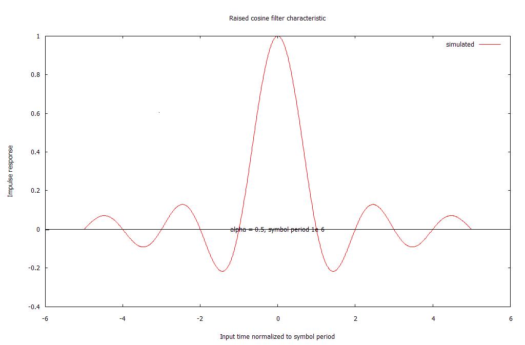
Further to the discussion of the raised cosine filter, a script was written to generate the impulse response of the filter. The results can be plotted for a graphical view using GNUPLOT as desired. The inputs are the symbol period, the roffoff factor, the number of symbol periods to be used in the calculation and the incremental time for the calculation. This script is also used in the design of the filter as is shown in the detailed design report to be presented. This report uses these scripts to design a digital FIR filter to implement the characteristic. The figure below shows the graphical result for the impulse response calculation using the script. Numerical data for the characteristic is available from running the script. Please visit http://www.signalpro.biz for more technical information.
Monthly Archives: May 2014
Raised cosine characteristic script result
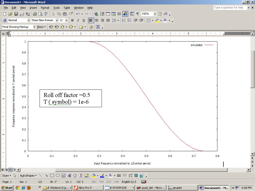
A script has been developed to analyze raised cosine filter characteristics. The input to the script is the symbol period and the roll off factor for the filter. In addition the frequency increment to be used for the calculation is also input. The program ( script) calculates the frequency response. The frequency respopnse is normalized to T the symbol period and the frequency is normalized to 1/symbol period. This blog also has other raised cosine information that can be found using the search function. The calculation results are plotted using GNUPLOT for easy viewing. An example plot is shown below. Please visit http://www.signalpro.bizfor more information.
Why use a filter for signals in digital communications
It is well known that Nyquist filters are used often in digital communications. A popular filter is the root raised cosine filter used both at the transmitting end and at the receiver. Together these two filters generate the raised cosine response which is what is needed. The obvious question that has to be asked is, why use these filters at all? The answer is that we use these filters because: (1) They slow down fast edges in the input signal so less bandwidth is required. Slower edges use less bandwidth. The filter smooths the edges of the signals. (2) At the receiver end the reduced bandwidth improves the sensitivity because more noise and interference is rejected. Please visit http://www.signalpro.biz for more information.
Root raised cosine filter
The raised cosine filter is a popular filter in the transmission and reception of digitally modulated signals. It is a class of Nyquist filter and provides a zero Inter-symbol interference ( ISI) property for digital pulses. However, in a usual communication system the combined path must have a raised cosine characteristic to take advantage of the raised cosine filter. In other words, the transmitter and receiver must implement this property. To do this the raised cosine filter is divided into two parts. Half of it is in the transmitter, and the other half is in the receiver. The product of the two halves must implement the raised cosine characteristic. To do this the actual filter characteristic that is implemented in each half of the filter is the root raised cosine filter. This filter response is simply the square root of the raised cosine filter. The complete response from transmitter to receiver will then be the correct response as desired.
Negative resistance
To understand negative resistance ( or conductance) we must define what positive resistance ( or conductance ) is. These primary elements act like absorbers of electromagnetic energy.Negative resistance ( or conductance) does almost the reverse. Negative resistance ( or conductance) does not actually generate energy. Rather they act to transform and release energy from a related source ( such as a battery ) into electromagnetic form. Negative resistance is defined as ” the property of a two terminal device with an internal source of energy which is controlled either by current through, or voltage across the terminals, but not by both”. Mathematically the difference between positive or negative resistance is illustrated by the slope at a point on a plot of the current – voltage characteristic of a device or system. The current is the ordinate and the voltage is the abscissa. If the current through the device or system increases with increased applied voltage ( positive slope) , then the sign of the slope is positive and the resistance is considered positive. If the current decreases with increasing applied voltage, then the slope will be negative. In this case the sign of the resistance ( or conductance ) will be negative i.e the device is a negative resistance ( or conductance).
Custom enclosures for electronics using 3 – D printing
It is interesting how 3 – D printing is changing the landscape when it comes to enclosures for electronics. Signal Processing Group Inc., has been using SOLIDWORKS to design and model custom enclosures for electronics. Once the enclosure is finalized a step beyond is to make volume copies of the finalized enclosure. An estimate of time it took to design and model a custom enclosure: 3 days. Time it took to print it out on a 3 – D printer: 3 – 8 hours. This allows rapid prototyping and is very cost effective. Please contact Signal Processing Group Inc., if you are interested in designing, modeling and printing enclosures for your electronics using SOLIDWORKS and 3 – D printing.
Logic design as an adjunct to analog/RF/wireless designs
Recent experience on the design of a transmitter/receiver pair at 915 Mhz was instrumental in prompting us to the utility of having a way to design small logic circuits quickly and simply. The peripheral circuits we were designing were small logic circuits using mostly the typical NAND/NOR/D-FF type circuits. In two cases we needed Schmitt triggers too, These were used at the inputs and to mitigate logic noise. CD 4000 was great for us. However the soldering and building of small boards was a tedious activity. I suppose gate arrays, CPLDs and FPGAs were meant to assist in this activity but these need all kinds of learning curves in software and programming. A new and more efficient type of digital device ( programmable) is needed which does not need multiple hours of programming and all kinds of special hardware for its use.
Interpolation filter in digital signal interpolation
Having been asked a really pertinent question about the previous post’s ( Interpolation ) description, this post is an attempt to answer it. The question: “If zero padding is the technique to be used in interpolation, and the inserted samples are zeroes, how does this work? Where do the intermediate sample values come from?” The answer to this question is, that the even though the inserted samples are zero, the interpolation filter is designed in such a manner that IT provides the missing samples. It interpolates between the available “true” samples of the old data stream and the new inserted zeroes to come up with the in – between samples. Please visit our website at http://www.signalpro.biz and click on the ” free articles …” menu item to access a broader description of multi-rate sampling.
Interpolation of digital signals: A very brief introduction
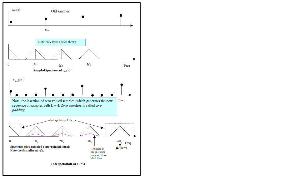
Interpolation in digital signal processing is a very interesting and useful technique. The fundamental idea is to change the sampling rate of a digital signal. The tedious way is to convert a digitally sampled signal into an analog signal using a digital to analog converter and then re-sample at a higher rate — i.e interpolation. A more elegant way is to actual perform interpolation directly on the digital signal. The graphical illustration of this is shown below.In this graphic the interpolation factor is 4. i.e the increase in sampling rate is 4X over the old sampling rate. The picture shows the zero insertion method of interpolation. As can be seen ( upon magnification of the picture ( click twice on it). a interpolation filter is also an integral part of the process. Also an input anti-aliasing filter helps by limiting the signal bandwidth. This is usually an analog filter. For more details on multirate sampling please visit our website at http://www,signalpro.biz and click on the free reports link and check out the multirate sampling report.
QPSK: I/Q modulator impairments and their effect on the receiver.
This is a short post that follows on to the last post about QPSK modulation techniques using a I/Q modulator. The description was based on idealized operation of the modulator in an effort to explain the operation. The real world effects were not explored. The fact is that I/Q modulators have at least two impairments that affect the accuracy of the transmitted signal. In order to explain this, note that the phase shifts in QPSK are also realized through the gain of the I/Q channels. Thus if there is an imbalance in the gain of the two channels then an error in the transmitted constellation will occur. If either the I or Q channel is imbalanced with respect to the other, the constellation will change from a square shape to a rectangular shape. If there are also phase errors then the constellation will change to a parallelogram and so on. These are the two most important impairments in the I/Q modulation scheme. Another impairment in the overall transmitter is the non-linearity of the final power amplifier. This will affect the constellation too. The white additive noise in the transmitter and the receiver will cause the received constellation to be spread out in the phase/gain space. Under worst case conditions the constellation may cease to exist and extreme loss of bit error rate will result. However, as far as impairments in the I/Q modulator are concerned, it may be a relief to know that modern day I/Q modulators have very low gain and phase errors. For example a well known device has a gain error of 0.12 dB and a phase error of 0.05 degree. In addition trimming of these errors can also be achieved using digital to analog converters and non volatile memory storage. The errors are trimmed out in the factory before final delivery.


