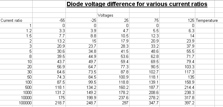
As presented in an earlier post, whenever currents pass through the base emitter junctions of two bipolar transistors, it leads to the generation of a differential voltage. This voltage is very useful in the design of circuits such as voltage references, translinear circuits etc. A javascript calculator that allows the calculation of this voltage is now available from the Signal Processing Group Inc website under “Complimentary Items”. Interested parties can download this calculator for free from the SPG website.
Monthly Archives: December 2014
Bipolar current ratios and differential voltages
The differential voltages generated by two currents passing through two bipolars generate a differential voltage that is useful in the design of various circuits such as voltage references, translinear circuits etc, In order to develop a quick reference guide to this, Signal Processing Group Inc., has released a useful table relating current ratios and differential voltages generated. This is shown below. Please visit our website for a lot of other useful information.
1 dB gain compression for input , for output and small signal gain relationship
Gain compression points are quoted often and easily in datasheets, specifications and elsewhere. However to really use this data one needs to know what these numbers allude to and how they can be used. To learn more about gain compression please refer to the post by Signal Processing Group Inc. ( at the following link: www.signalpro.biz/pointsf1.pdf ). However this post simply reiterates the relationship between the input 1 dB compression point, the output 1 dB compression point and the small signal gain. The expression is: Pin( 1 dbCP) in dBm =Pout(1dbCP) in dBm- [gain(db)-1] ( in dBm). So if the output compression point is known one may back calculate the input 1 dBCP using the small signal gain of the device. ( or vice – versa).
RMS jitter calculation from phase noise power
It is obvious, that time-frequency duality indicates, that phase noise can be converted to rms jitter. Phase noise is usually measured in terms of dBc/Hz where the “c” indicates with respect to the power of the carrier. Once this measurement is done it is possible to convert the phase noise between frequency limits to rms jitter using the following formula: rms phase jitter ( in radians) = sqrt [ 2.0*10** (A/10)]. Here ** indicates exponentiation. A is the power in dBc over the band. This is simply the area under the phase noise curve.(If the jitter is to be used in terms of seconds, divide by 2*pi*fo, where fo is the oscillator center frequency). A number of good routines are available freely on the web to calculate the area under the noise power curve. (To read about the phase noise please visit http://www.signalpro.biz/register.html and select the oscillator noise paper…)This identity is embodied in the jitter calculator that can be accessed from the Signal Processing Group Inc website from the free items link.


