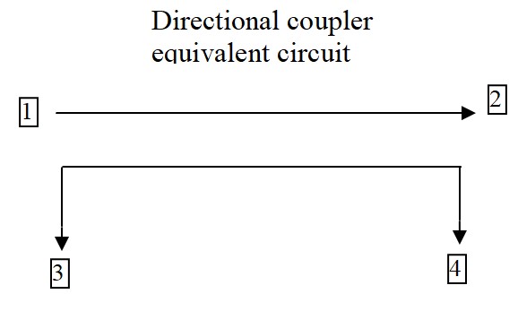
The DIRECTIVITY of directional couplers is an important parameter when using a coupler. Simply defined it is the ability of the coupler to distinguish between forward and reverse signals. Referring to the diagram below, we can define the directivity as:
D = s31 + s21 – s32. where s31=coupling ratio, s21=insertion loss and s32 = isolation. All these are defined negatively in dB, but D itself is stated positively. A shorter form is also used for forward measurements as D = s31 – s32. The question is: why is directivity important?
To elaborate a little: power is applied to port 1 and output at port 2. Some of the applied power is coupled to port 3 with a coupling factor of K^2. At port 3 part of the input power is sampled. Port 3 is the coupling port. Port 4 is the isolation port where ideally, no input power should appear. Any of the ports can be defined as the input port provided the other ports are appropriately labeled.
Mathematically speaking we can define: Coupling = 10Log(P1/P3) = -20LogK ( dB). Also in a similar fashion the other parameters can be defined: Directivity = 10Log(P3/P4) = + 20Log[K/ABS(s14)]. Isolation = I = 10Log(P1/P4) = -20Log[ABS(s14)] dB. Insertion loss = L = 10Log(P1/P2) = -20Log[ABS(s12)] dB.
The coupling shows how much of the input power is coupled to port 3. The directivity shows how well the coupler isolates forward and reverse signals. Isolation shows how much of power is delivered to the isolated port. The insertion loss provides the calculation for the amount of power delivered to the output port, less the power delivered to the coupled and isolated ports. In an ideal coupler the directivity and isolation are infinitely high.
Using the example of measuring an unknown impedance with a signal source, a detector and a coupler, we see that if the unknown impedance is perfectly matched to the source impedance then there is no reflection of power at all, and there is no reverse wave. So in this case we will measure the impedance perfectly. Its simple enough ! However, if the unknown impedance is not matched to the source impedance then there will be a reflected wave. We sample this using port 4. In this case however, the coupler not being ideal will transmit part of the reverse signal to port 3, the coupling port that we also use to sample the forward signal. Now there will be an error in the measurement. We need as little of the reverse signal in the coupling port as possible. A characteristic of the coupler. This is why directivity is important. The higher the directivity the less error we will get. A very good article on this topic is provided by REF1: ” Directivity and VSWR measurements”, by Doug Jorgesen and Christopher Marki of Marki Microwave Inc. They also provide curves of error versus directivity etc. A very readable article. Please visit our website for more articles of interest, calculators and a description of what we do and some of our products.


