A current source digital to analog converter is inherently fast. It can be implemented in most semiconductor technologies. This post and its accompanying article/ white paper describes one such DAC that uses a 0.18um CMOS technology ( decidedly legacy in semiconductor terms) but its assessments are equally applicable to latest CMOS technology. The various analysis for circuit, performance, power etc. etc can be used as a template with appropriate modifications for any CMOS process. Please visit the Signal Processing Group Inc., website to access the full white paper that can be found under the “complementary” menu.

Monthly Archives: April 2021
3D modeling and printing for electronics/mechanics
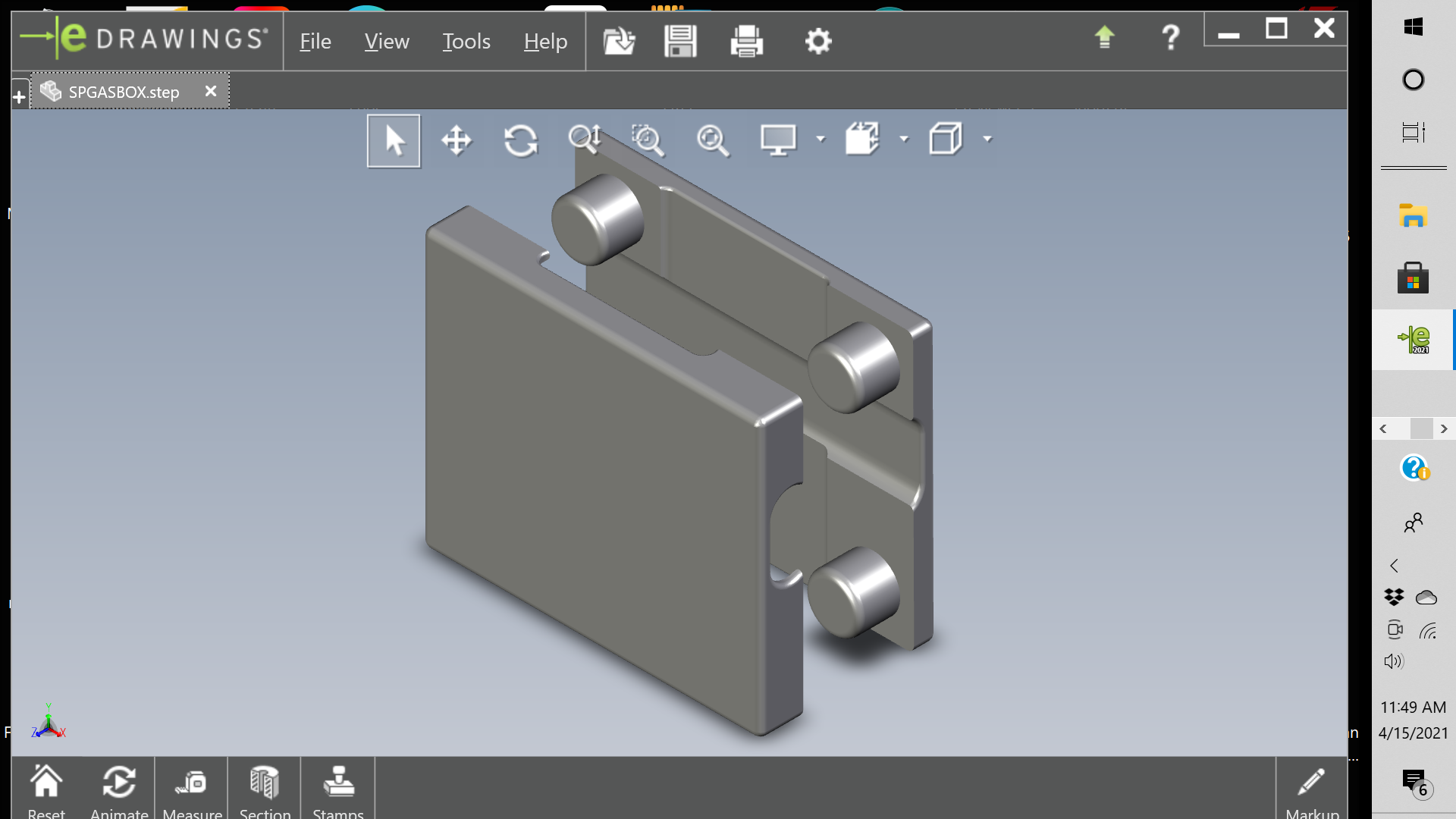
3D design and modeling has come a long way in the last few years. At Signal Processing Group Inc. we are using it to our advantage (and our customer’s advantage) to design, model and print enclosures and more. ( An example of a simple enclosure is shown below). A number of CAD tools ( Solidworks, Shaper3D, etc) have come up that allow this 3d design to be done. Young designers graduating from design schools like The Art Center in Pasadena, California are making inroads into the design world and are available to work for businesses/individuals to produce beautiful designs for spacecraft to pencils and everything in between. A particularly interesting application is in medicine and biomedicine. Robotics is benefiting greatly from this art/technology too. I believe this is going to be a technology that will serve us well in the coming years and its advance can be fairly well predicted. Please contact Signal Processing Group Inc. if you would like to get going in 3D technology and printing.
Charge pump PLL design analysis for a 0.18um CMOS process
A charge pump PLL is a popular way to design a PLL. It is a good idea to analyze its requirements and relate the design to those parameters even before the functional blocks are designed. This provides the design engineer a pathway to complete the design from behavioral modeling to a final semiconductor layout to be fabricated. The higher level analysis can be done very quickly and lays bare the techniques, risks, timelines etc. for the design. A recent whitepaper by Signal Processing Group Inc. presents these assessments. The article can be found under the complementary menu in the SPG website. Please visit the SPG website for this and other articles of interest.