2019 has dawned with so much promise. Looks like some really interesting conferences coming up too. The CES and the IMS conference in Boston. At SPG we continue our work on RF/Microwave and specialized APPS. Amplifiers, LNAs, mixers, oscillators, detectors, 902-928 filters ( SAW based) etc. Our service business is in full swing and we are not only designing products but also doing measurements, performance verification, testing etc. Our website is finally under construction as we attempt to modify it. Currently 4 books on Impedance matching have been published and are available on Amazon. All books authored by Ain Rehman. More informational products on RF/Microwave and analog hardware and APPS are in the works. Looking forward to your continued custom like years past. Please visit the website at spg@signalpro.biz.
Author Archives: Ain
Voltage to current converter for a grounded load.
My recent experience in searching for information on this topic on the web was fairly negative. The reason for the search was to use a translinear circuit in my system design. Translinear circuits work on currents so a voltage to current converter is required at the input. ( Perhaps a current to voltage converter on the output. Simplest being a resistance). There is not a lot of information on V to I converters on the web specially if you are looking for a simple one. I found one that seemed to be popular and simulated it on LTSPICE. Its quite complicated and uses an opamp or two. Still searching for a simpler one which would be compatible with device level translinear circuits. Ultimately looks like I may need to design one. 
Volterra series
The Volterra series is a mathematical tool to model RF amplifiers with memory and in general, any non linear system with memory. In many ways the Volterra series is analogous to the Taylor series for systems with no memory. The Taylor series has coefficients multiplying each power of the independent variable. The Volterra series has “kernels”. Volterra kernels are difficult to calculate beyond the third order so most analysis only uses that as the maximum limit in analysis. The Volterra series was used to develop the behavioral model of a RF power amplifier. Please visit the SPG website for more articles and items of interest.
Impedance matching using single stubs
A new book was published that describes the process of using a single stub to match a load with a transmission line. The method is simple but requires some understanding. This book describes the methodology, presents an example and presents a completely simulated design using easily available public domain tools. The book can be purchased from Amazon. To browse follow this link:https://www.amazon.com/s/ref=nb_sb_noss?url=search-alias%3Daps&field-keywords=impedance+matching+using+single+stub
Please also visit the Signal Processing website for more items of interest.
Cascaded line matching of impedance with ideal transmission lines simulation.
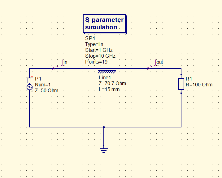
A cascaded transmission line is one of the simplest ways to match impedances. It is simply a quarter wave transmission line with a characteristic impedance given by : Z0 = sqrt(ZS.ZL) where ZS is the source impedance and ZL is the load impedance. A simulation using a public domain simulation CAD tool was performed for s11. The result is shown below:
From the figure the frequency was 5 Ghz. The schematic of this design is shown below:
Note that the impedance of the line is: sqrt(50*100). The length of the line is a quarter wavelength ( 1 wavelength = 60 mm at 5 Ghz).
For more information on impedance matching please refer to the available book : “VSWR and Impedance matching techniques”, available from Amazon,
In addition a forthcoming book that includes many other techniques and scripts is in preparation.
Please visit our website for more information on our offerings and more technical information/articles.
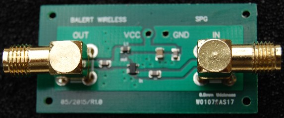
A low noise amplifier module with NF = 1 dB across the 100 Mhz to 3.0 Ghz band with typical 17.7 dB small signal gain over the band.
Bipolar switching circuit performance parameters
As analog engineers focus on parameters such as the transition frequency of a bipolar device to estimate frequency performance of a transistor ( which is more of a small signal parameter). We sometimes get confused if we have to use a bipolar as a switching device. Especially in a saturated mode of switching. In this case the base of the bipolar is driven hard enough ( lots of base current) to drive the transistor when it is ON to store charge in its base region. The output voltage at the collector drops to its Vsat ( a few hundred millivolts usually) and when the transistor has to leave this state it has to contend with a storage time. So when we want to estimate the switching speed of a bipolar we need to use the datasheet parameters of the device that apply to the switching mode. These parameters are: td = delay time , tr = rise time, tf = fall time and ts = storage time. Then the maximum switching frequency of the bipolar is given by ( estimate), fmax=1/( td+tr+tf+ts). Note that ft, the transition frequency does not enter into this equation at all! For more technical info and services please visit our website.
RFMW design: Comparing Characteristic impedance results for a microstrip from multiple calculators
We took 4 different available calculators and compared results obtained for Zo on a PCB microstrip. Results were that the SPG package and APPCAD results were very close, TXLINE results were larger than the SPG and APPCAD results, while the wCalc package was lower than the SPG and APPCAD numbers. (wCalc does provide some very valuable parameters as a result of the simulation: R, L, C and G parameters for the microstrip). Here are the comparisons.
Please visit the SPG website for more information and reports.
Using a directional coupler to measure an unknown impedance
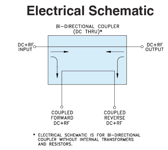
Lets measure RL (return loss) using a bi-directional coupler. In this case we are using the BDCN-20-13+ from Mini-Circuits For this coupler key parameters are:
Coupling port power 20 dB, Directivity 12 dB. Main line loss between 370 Mhz and 470 Mhz is 0.25 dB max. Characteristic impedance is 50 Ohm
Ports are :
1 – the input port
4 – output port
6 – coupled port in the forward direction
3 – coupled port in the reverse direction
Now to further our analysis lets connect a load to port 1 and drive port 4. So this is a reverse direction operation for this coupler.
To use some numbers, lets input 0 dBm at port 4. Then since the loss on the mainline is 0.25 dB the power arriving at port 1 is -0.25 dBm. Also:
lets assume the load is exactly 50 Ohm and we terminate port 3 with also 50 Ohm. Now the power coming out of port 6 is -32 dBm if the coupler is ideal. (directivity + coupling ).
Now lets assume that the load is no longer 50 Ohm but 100 Ohm. Now there will be reflected power also being added to the power out of port 6. The difference between the
– 32 dBm and the total power being measured at port 6 with 100 Ohms is the reflected power PR.
Then the return loss is simply
RL=10log10(PT/PR) dB.
Here PT is 0 dBm. Once RL is known other parameters can be calculated.
Directivity of Directional Couplers: another look.
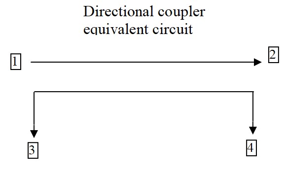
The DIRECTIVITY of directional couplers is an important parameter when using a coupler. Simply defined it is the ability of the coupler to distinguish between forward and reverse signals. Referring to the diagram below, we can define the directivity as:
D = s31 + s21 – s32. where s31=coupling ratio, s21=insertion loss and s32 = isolation. All these are defined negatively in dB, but D itself is stated positively. A shorter form is also used for forward measurements as D = s31 – s32. The question is: why is directivity important?
To elaborate a little: power is applied to port 1 and output at port 2. Some of the applied power is coupled to port 3 with a coupling factor of K^2. At port 3 part of the input power is sampled. Port 3 is the coupling port. Port 4 is the isolation port where ideally, no input power should appear. Any of the ports can be defined as the input port provided the other ports are appropriately labeled.
Mathematically speaking we can define: Coupling = 10Log(P1/P3) = -20LogK ( dB). Also in a similar fashion the other parameters can be defined: Directivity = 10Log(P3/P4) = + 20Log[K/ABS(s14)]. Isolation = I = 10Log(P1/P4) = -20Log[ABS(s14)] dB. Insertion loss = L = 10Log(P1/P2) = -20Log[ABS(s12)] dB.
The coupling shows how much of the input power is coupled to port 3. The directivity shows how well the coupler isolates forward and reverse signals. Isolation shows how much of power is delivered to the isolated port. The insertion loss provides the calculation for the amount of power delivered to the output port, less the power delivered to the coupled and isolated ports. In an ideal coupler the directivity and isolation are infinitely high.
Using the example of measuring an unknown impedance with a signal source, a detector and a coupler, we see that if the unknown impedance is perfectly matched to the source impedance then there is no reflection of power at all, and there is no reverse wave. So in this case we will measure the impedance perfectly. Its simple enough ! However, if the unknown impedance is not matched to the source impedance then there will be a reflected wave. We sample this using port 4. In this case however, the coupler not being ideal will transmit part of the reverse signal to port 3, the coupling port that we also use to sample the forward signal. Now there will be an error in the measurement. We need as little of the reverse signal in the coupling port as possible. A characteristic of the coupler. This is why directivity is important. The higher the directivity the less error we will get. A very good article on this topic is provided by REF1: ” Directivity and VSWR measurements”, by Doug Jorgesen and Christopher Marki of Marki Microwave Inc. They also provide curves of error versus directivity etc. A very readable article. Please visit our website for more articles of interest, calculators and a description of what we do and some of our products.
RF Transformer: Relationship between the primary and secondary inductances with the turns ratio
The transformer primary and secondary inductance ratio is equal to the square of the turns ratio of the RF transformer. Simple, but useful identity for multiple applications and specifications. So Ls/Lp= N*N where N is the turns ratio of the transformer. Please visit our website for more information about us and other items of interest.

