Class F RFPA design: Waveforms of the amplifier

A class F amplifier is highly efficient and uses waveform shaping at the drain of a power device. This shaping takes the form of using ( usually) the second and third harmonic of the waveform to generate a drain to source ( collector to emitter) voltage that is roughly a square wave ( ideally a square wave, but we all know that ideal is a not a word we can use loosely). The drain current is then shaped to be very small when the D/S voltage is high and high when the D/S voltage is low. This causes a non-overlapping condition in operation and ensures a high efficiency. A pre-distortion or pre-conditioning circuit is also required to get the desired linearity. ( This is the subject of a later post). The waveforms below are what we got using Microwave Office as the simulator. The active device was a Cree 40010. It is simply instructive to examine the waveforms in case the reader is starting to design a Class F. The figure below represents the drain source waveform.

The figure above is the D.S current in mA.

The figure below is the simulated power gain and PAE.

We hope these will be of help to aspiring designers of Class F amplifiers. Please visit the Signal Processing Group Inc., website for more information and articles of interest.

RF/Microwave design: The spacing circle in double stub matching

The Spacing Circle in double stub matching

In double stub matching the two stubs are spaced a predetermined distance away from each other. These distances are typically λ/8, λ/4, 3λ/8, 5λ/8 etc. Knowing what we know about a length of line acting as a transformer, we know that the length of line between the two stubs acts as a transformer. The action of this transformer is to convert the admittance at the position of stub 2 to a different admittance at the position of stub 1. So we start from the position of stub 2.

In order that stub 2 can be finally used to match the line admittance, the real part of the admittance at the position of stub 2, on the line, has to be 1.0 (normalized value). Its susceptance is then jB. jB is the susceptance that is cancelled using stub 2 to ultimately get the matching to the line admittance. The admittance at the position of stub 2, (without the stub) lies on the constant conductance, g = 1 circle. The admittances on the g = 1 circle are all the possible admittances at the stub 2 position for a match to take place.

To reiterate, as a result of these deliberations, that some point of the VSWR circle formed by the position of stub 2, must intersect the g=1 or the unity conductance circle on the Smith Chart.

We also conclude, that the admittance at the position of the first stub, must lie on
a circle of equal radius but having its center rotated (moved to or displaced) by the spacing between the stubs towards the load. Lets call this spacing ‘d’.

This circle is called the spacing circle.

Please visit our website for more articles of interest.

Analog design and test: using older testers in new ways

Its interesting how really old digital or mixed signal testers can be used in new ways with a good loadboard. I do not know how many engineers remember the old IMS tester. Its really old but with proper care and maintenance still provides good service. Its basically a digital tester but there are options that allow it to operate as a mixed signal or analog tester. Even a digital only tester can be used as a high frequency analog/RF tester with  the proper load board. The high frequency – digital interface resides on the loadboard. The tester then is used in its standard capacity as a digital tester. The interface takes care of the RFMW/Analog interface. Interesting. Please visit our website for more articles of interest, products and services offered.

SPG delivers great services. Please contact us at spg@signalprop.biz

Filter design: SAW filters for precise filtering. Some thoughts

SAW filters can be a great way to get precise filtering done at reasonable cost ( $1.0 – $2.00 for 915 Mhz, 26 Mhz B.W. filter). However, they do need to be handled with respect as they are ESD sensitive devices. A good app note can be found at http://www.mouser.com/pdfdocs/ESDProtectionforSAWFilters.pdf for interested parties. Check out our website for more info and our services.

SPG designs, develops and delivers custom analog and RF/wireless asics and modules.

Comparison of the characterisitic impedance of PCB lines using the SPG calculator, TXLINE and APPCAD calculators.

A comparison was done for results obtained using the Signal Processing Group Inc., characterisitic impedance calculator, the NI TXLINE calculator and the APPCAD calculator. The results are: SPG calculator -> 71.4 Ohms, TXLINE->79.47 Ohms and APPCAD -> 68.96. Please visit our website for more information about us and more technical articles.

RFMW design: Comparing the leading CAD tools, ADS ( Keysight) and Microwave office ( NI) for RFPA design.

Recently evaluation verisons of ADS and Microwave Office were used to evaluate an existing 10W Class F RFPA design. The active device was a CREE 40010 packaged  part. Here are my the insights at first blush. ( Other users will probably have a vastly different experience). Both tools are very good and provide excellent solutions to a difficult problem. However,

( 1 ) Technical support on MWO was excellent. Questions were answered and much more. ADS technical support was sluggish and difficult to get to.

(2) Model installation in ADS was extremely easy while that in MWO was a little messy and took a long time.

(3) License file installation was very easy in ADS and fairly involved and difficult in MWO.

(4) LineCalc on ADS was very good and provided accurate results. TXLINE in MWO was less so and needs some improvement.

(5) Running two tone simulations was very easy on ADS and quite difficult on MWO. However MWO provided a more flexible interface and experienced MWO users will probably like it more. ADS has a somewhat more limited tool.

(6) Help on ADS was marginally better than MWO, and provided more explicit answers than in MWO.

(7) Up and running time was short on ADS and long on MWO.

(8) Examples on ADS were marginally better than in MWO and provided more details and help.

(9) MWO marketing/sales support was simply superb and very obliging. ADS sales support was very slow and in some cases non-existent.

(10) MWO has a much better stable of CAD tool routines than ADS. This allows a more flexible approach to analysis.

(11) ADS has a better user interface for output results that includes both textual and graphic output accesses with ease.

(12) Not enough evaluation time was provide to go into EM and layout eval so these are not addressed in this post.

To conclude: For someone getting into RFMW analysis tools ADS may be a better choice initially but much less flexible and somewhat limited CAD tools. MWO is for the more experienced user, but its limitations are compensated by the level of and quality of the technical and sales/business support. Please use our website at www.signalpro.biz for contact or for comments or for more information about our services.


Double stub impedance matching for RF and Microwave design


Its interesting how many techniques exist today for impedance matching of complex loads to transmission lines. A really interesting one is the technique of double stub matching which is a popular one. Its simpler cousin is single stub matching which can be used but runs out of steam under some circumstances

Double stub impedance matching is more involved than single stub matching. First of all we need to discuss the rationale for using double stub matching. In order to understand all this, consider the points below:

1.0 A single stub match involves the use of a stub of fixed length placed at a fixed position on the transmission line from the load for a specific load.

2.0 If the value of the load changes then the length of the stub and the position at which it is placed must also change.

3.0 A better technique would be where we could fix the positions of the stubs in relation to each other and only change the lengths of the stubs to match varying loads. This is done using the techniques of double and triple stub matching.

4.0 Both analytic and graphical techniques are available to do double stub matching. The graphical method is usually the Smith Chart method and that is what we have focused on. However analytical techniques can be enlightening as well, and are recommended if you are mathematically minded.

5.0 In order to further understand the technique of double stub matching you need a reasonable amount of the understanding of how the Smith Chart works.

6.0 There are some loads that cannot be matched using double stub matching by simply altering the length of the stubs. However if we are willing and able, to move the stubs together a distance away (or towards the load) from the load then we can accommodate the load. This can be discussed and illustrated using the Smith Chart method. These loads form an area of the Smith Chart collectively known as the forbidden zone for double stub matching.

7.0 Additional techniques can be used to overcome the limitations of double stub matching if needed. Similar techniques to that of double stub matching are used for triple stub matching.

The interesting situation as far as learning about double stub matching is that there are very few articles available that really discuss the technique for the newbie. We know as we did a web search and came up with very few articles that deal with this.

A forthcoming book from Ain Rehman of Signal Processing Group Inc, addresses these techniques in some detail with a minimum of math. The title is VSWR and Impedance matching techniques. This book will be available on Amazon both as a paperback and as a Kindle book shortly for interested readers.

Please visit our website www.signalpro.biz for more information and other articles of interest.

Signal Processing Group Inc., delivers RF Design, RF IC design, rf circuit design, ic design, analog design, rf technology, analog circuit design, asic chip, integrated circuit design and various rf devices

This is low noise RF Amplifier by Signal Processing Group Inc., available from Amazon

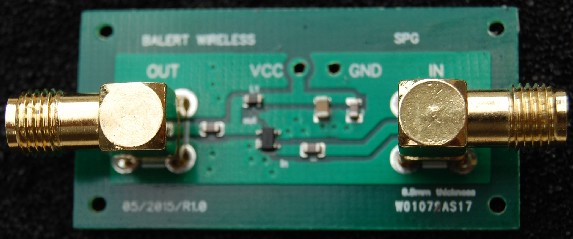
A low noise RF amplifier by Signal Processing Group Inc.
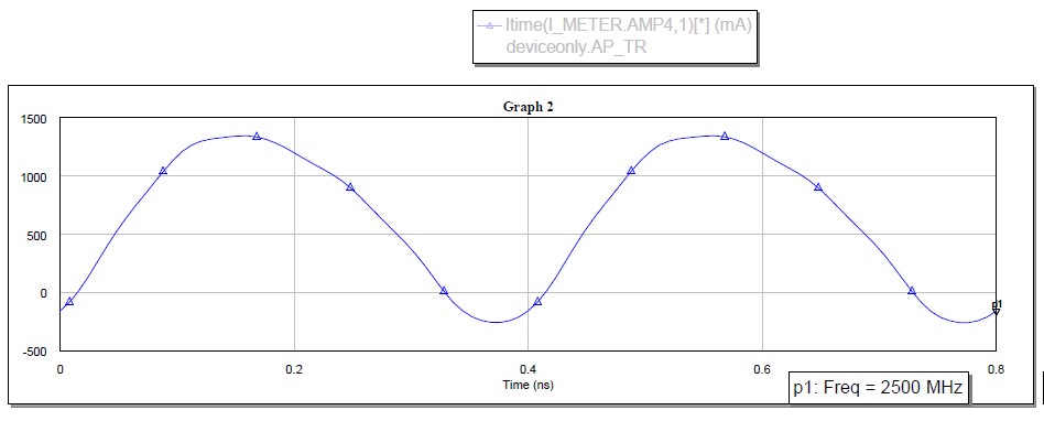
SPG designs, develops and delivers custom analog and RF/wireless asics and modules.

RF/microwave design freeware

Its so impressive to see the amount of freeware now available to do RFMW design and development. From the “free-est” of freeware for RFMW ( APPAD) to many other packages. A harmonic balance tool is also available as freeware. The consequence is that we as design engineers do not always have to pay an arm and a leg to get the commercial packages ( of which there are few) and be hostages to these vendors. A lot of work can be done prior to spending umpteen dollars so that the cost can be lowered significantly.  Currently we have a few of these freeware tools under assessment and will be reporting on their performance in this blog.

RF/Microwave design: The inductance and capacitance equivalents of microstrip/transmission lines


Microstrip ( or transmission lines) are used extensively in high frequency design of MMICs or PCB level circuits. In many cases it is simpler just to use a piece of microstrip as an inductance or a capacitance. ( Especially in microwave design). However we need to calculate what the microstrip dimensions should be to realize an inductor or a capacitor or both. ( There is much more information in the second edition of the forthcoming book on VSWR and matching techniques for the interested reader). Here then are the expressions for these types of structures:

XL = reactance of an inductive line = XL= ZoSin( 2*pi*length/lambdag). From this expression one can extract what the length should be as well. Here length is the length of the microstrip ( generally higher resistance e.g 100 Ohms), lambdag = wavelength in air/square root ( relative permittivity) also known as guide wavelength in some texts. Zo is the characteristic impedance of the microstrip line.

Capacitors can also be realized by microstrip structures. In this case the susceptance is given by:

B = (1/Zo)Sin2.0*pi*length/lambda. It should be noted that the line lengths for a capacitance are usually short and of low impedance.

In each of these structures there are accompanying parasitic elements also, In the case of an inductance there are parasitic capacitors at the two ends. forming a pi circuit, See the diagrams below. In the case of a capacitor there are series inductances in its leads,

Please see the reference on these expressions: Foundations of Interconnect and microstrip design by T.C Edwards and M.B Steer. John Wiley and Sons LTD, publisher.

For more and other interesting information and articles visit our website.


Integrate a board based prototype design using SPG's custom design and delivery services

RF Power amplifier design: small signal and large signal s-parameter comparison

Small signal s parameters are a well known set of parameters in small signal RF amplifier design. However, if the amplifier is a RF Power amplifier then small signal s parameters will not accurately reflect its operation. In this case large signal s parameters are required. So what is the difference in values between small signal s parameters and large signal s parameters for a particular circuit? To answer this question we ran a simulation using a well known industry standard simulator to derive both small signal and large signal s parameters at a particular frequency and particular bias conditions. The results are shown below.

The frequency is 2.5 Ghz. The small signal parameters found were: s11=0.184/-45.56, s12=0.019/-37.358, s21=4.306/24.992 and s22=0.465/35.422.

The large signal s parameters at the same frequency were: s11=0.691/13.914, s12=0.148/11.864, s21=0.148/11.864 and s22=0.965/-170.913.


Please note the difference Please visit our website for more articles and information.