This post by Ain Rehman. Looking through the literature a HEMT model that seems to be understandable and useful for hand calculations seems to be the Chalmers model. It is intuitive and resembles the familiar MOSFET type models that designers have been used to. Signal Processing Group Inc.is in the process of developing some useful relationships from this model that can be used for simple first order calculations for design. These relationships will be tested thoroughly and all assumptions validated. At the conclusion of this exercise a set of equations will be presented that will allow hand calculations to be made, to within a reasonable degree of accuracy as a starting point of a HEMT ( or pHEMT ) circuit design. Please visit our website for other technical information and our service and product offerings.
Category Archives: Uncategorized
HEMT/pHEMT absolute basics
HEMTs and pHEMTS are important new semiconductor devices that have a high performance profile. They are also low noise. GAN HEMTs are being used in high power RFMW power amplifiers. pHemts are also being used in high frequency and low noise amplifiers. The operation of the HEMT is not immediately intuitive. This post seeks to provide a basic description of the backbone of the HEMT operation. Following posts will explore more details of the HEMTs/pHemts. Interested parties may access a detailed description from the Signal Processing Group Inc., website under the “complemntary items ” menu.
Bipolar transistor noise: The equivalent noise resistance
A large number of very detailed noise analyses are available for bipolar noise and some of them are very detailed indeed. However, for a quick design assessment of noise it is more useful to use the bipolar equivalent noise resistance. This is given by : RN = rb + 1/2gm. Here rb is the base series resistance and gm is the transconductance. What this expression is telling us is that to minimize noise use a stripe geometry for the bipolar to reduce rb and increase the current to increase gm. However, in the case of variable gain amplifiers this is a challenge to say the least. Most variable gain bipolar amplifiers use a varying gm. So as the current changes in the device the nose resistance also changes. A compromise has to be made.
Microwave amplifier design: Single stage gain calculator
A microwave single stage gain calculator has been developed by SPG to enable quick calculations of microwave amplifier gain stages. A set of s parameters for the active device/devices is required.
These parameters are inserted into the javascript calculator. The calculator allows the assessment of the gains to be made rapidly without the need of a lot of tedious hand calculations. Please access the calculator from the SPG website under the complementary items menu.
Microwave amplifier design: Single stage gains
This is a tutorial description of the calculations for single stage microwave gains using s parameters. Allows one to see what the ramifications of using I/O impedance and matching is to the gain obtainable from a microwave device.
There are multiple gains that must be taken care of including power gain, available gain, transducer gain, unilateral transducer gain etc. Associated with this tutorial is a javascript calculator to quickly assess the performance of the device so long as the s parameters are known. This will be presented in a subsequent post. The calculator will be available for free use.Please visit the SPG website and check under the complementary menu item ( Use cntrl – F ) for single page search for convenience.
Noise Figure to Noise Temperature converter
Noise figure and noise temperature are related quantities. Which one is used depends on the application and the context. A noise figure and noise temperature calculator is now available on the Signal Processing Group website, under complementary items for interested users. For quick reference here is a table of converted values.
| NF(dB) | T (K) | NF(dB) | T (K) |
| 0.1 | 7 | 2.1 | 180 |
| 0.2 | 14 | 2.2 | 191 |
| 0.3 | 21 | 2.3 | 202 |
| 0.4 | 28 | 2.4 | 214 |
| 0.5 | 35 | 2.5 | 226 |
| 0.6 | 43 | 2.6 | 238 |
| 0.7 | 51 | 2.7 | 250 |
| 0.8 | 59 | 2.8 | 263 |
| 0.9 | 67 | 2.9 | 275 |
| 1.0 | 75 | 3.0 | 289 |
| 1.1 | 84 | 3.1 | 302 |
| 1.2 | 92 | 3.2 | 316 |
| 1.3 | 101 | 3.3 | 330 |
| 1.4 | 110 | 3.4 | 344 |
| 1.5 | 120 | 3.5 | 359 |
| 1.6 | 129 | 3.6 | 374 |
| 1.7 | 139 | 3.7 | 390 |
| 1.8 | 149 | 3.8 | 406 |
| 1.9 | 159 | 3.9 | 422 |
| 2.0 | 170 | 4.0 | 438 |
RF/Analog ASIC design: Simple rule to calculate MOSFET flicker noise.
Last post dealt with MOSFET flicker noise. See:http://www.signalpro.biz/wordpress/analog-asic-design-a-mosfet-flicker-noise-calculator/. The calculator allows the user to calculate the flicker noise of a MOSFET using a relatively simple noise equation. This also leads to a rather simple rule and expression for the calculation of flicker noise. The expression states: rms noise/root Hz = AN/WL. Here W is the width of the MOSFET and L is the length of the MOSFET. AN is constant AN can be calculated by using the calculator. This allows simple calculations for various MOSFETs based on their gate area. The message is clear. If you want a low flicker noise then increase the gate area of the MOSFET. The calculator can be accessed from the Signal Processing Group Inc., website.
Check out our RF amplifier products
Take a look at the custom ASIC/module services offered by Signal Processing Group Inc. Click on the image below
Check out this book on impedance matching,
Analog ASIC design: A MOSFET flicker noise calculator
1/f noise in MOSFETs is a subject for continual study. Multiple noise models have been derived and studied. Each of these have some advantages and disadvantages. At SPG we have used a simple model of 1/f MOSFET noise for some time. It has served its purpose in allowing us to at least estimate the 1/f noise for our design purposes. By using some kind of thumb rule, most appropriate to a particular design it is quite possible to use this model effectively. The model is presented below with credit to the source. The calculation based on this model has also been coded into a javascript that is available for the user. The original author of the paper is: Chorng – Kuang Wang. This model is further described in a Memorandum No. UCB/ERL M79/78 issued by UC Berkeley. Please visit the Signal Processing Group Inc., website to acces the script. The link can be found under :”Complementary” items.
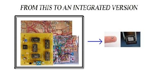
If you are interested in developing a custom analog chip or a RF IC please check out our custom design services by clicking on the image below.
Check out our RF amplifiers. Click on the image below.
Microwave amplifier design: Calculate the modified output reflection coefficient using s parameters
When a two port network, typically a microwave amplifier,is terminated in load and source impedances the input and output reflection coefficients are modified. The output reflection coefficient, TOUT is calculated using s parameters, the input termination, ZS and the output termination ZL. In addition the characteristic impedance of the microstrip or transmisson lines is also required.. Signal Processing Group Inc., has developed simple calculators to do this. A calculator for TIN and TOUT are both available on our website and may be accessed from the complementary items menu.
RF amplifier, HF amplifier, RF amp, low noise amplifier, microwave amplifier, broadband amplifier and amplifier module products from Signal Processing Group Inc.
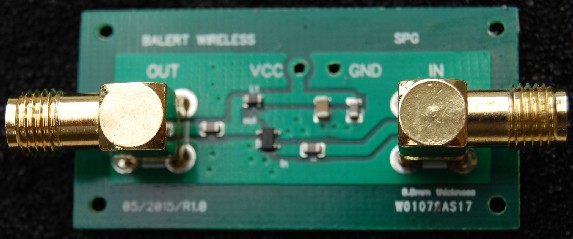
RF amplifiers, be they just a RF amplifier, a HF amplifier, a RF Amp, a low noise amplifier, a microwave amplifier, a broadband amplifier or RF amplifier modules are incredibly useful items. Currently Signal Processing Group Inc., has designed, developed and is delivering these types of amplifiers. Interested parties can simply, either purchase them from the SPG website or from a online store like Amazon. Please go the RF amplifier page and check out the SPG offerings.

A low noise RF amplifier by Signal Processing Group Inc. Please click on the image to check out other RF amplifiers from SPG
Please note that high volume supply is available with an increased lead time. Please contact us for volume deliveries on spg@signalpro.biz or call 866-487-1119.
In addition,full custom RF amplifier design is available to our customer’s specifications. Please contact us with summary specifications for a budgetary quote at no cost.


