Gain compression points are quoted often and easily in datasheets, specifications and elsewhere. However to really use this data one needs to know what these numbers allude to and how they can be used. To learn more about gain compression please refer to the post by Signal Processing Group Inc. ( at the following link: www.signalpro.biz/pointsf1.pdf ). However this post simply reiterates the relationship between the input 1 dB compression point, the output 1 dB compression point and the small signal gain. The expression is: Pin( 1 dbCP) in dBm =Pout(1dbCP) in dBm- [gain(db)-1] ( in dBm). So if the output compression point is known one may back calculate the input 1 dBCP using the small signal gain of the device. ( or vice – versa).
Category Archives: Uncategorized
RMS jitter calculation from phase noise power
It is obvious, that time-frequency duality indicates, that phase noise can be converted to rms jitter. Phase noise is usually measured in terms of dBc/Hz where the “c” indicates with respect to the power of the carrier. Once this measurement is done it is possible to convert the phase noise between frequency limits to rms jitter using the following formula: rms phase jitter ( in radians) = sqrt [ 2.0*10** (A/10)]. Here ** indicates exponentiation. A is the power in dBc over the band. This is simply the area under the phase noise curve.(If the jitter is to be used in terms of seconds, divide by 2*pi*fo, where fo is the oscillator center frequency). A number of good routines are available freely on the web to calculate the area under the noise power curve. (To read about the phase noise please visit http://www.signalpro.biz/register.html and select the oscillator noise paper…)This identity is embodied in the jitter calculator that can be accessed from the Signal Processing Group Inc website from the free items link.
RF Transformer, impedance ratio proportionality to voltage ratio
When using a RF transformer, remember that the supplier specifies the impedance ratio of the transformer. The relationship of the impedance ratio to the voltage ratio of the transformer is:
20log[sqrt(Output impedance/input impedance)] = 20log(output voltage/input voltage). The currents are inverse 20log(Input current / output current)
Chip resistor frequency performance considerations for RF design
As frequencies increase the chip resistor capacitance, inductance and pad parasitics start playing a significant role in the performance of the resistor . Sometimes at higher frequencies a chip resistor may start behaving capacitive sometimes inductive. A Signal Processing Group Inc., high frequency product was to be designed using chip resistors of value 75 Ohm. We investigated the chip resistor frequency response and found that for the highest frequency response the 0201 size is the best. However, assembling 0201 is quite challenging. The next best choice is 0402. This too has its difficulties in assembly. Going further down is the 0603 size, which is easier to use but has poorer frequency response generally than the 0201 and 0402 sizes. However, in our case the resistor value was 75 Ohm. From looking at the characterizations done by a well known chip resistor vendor it appears that if the resistor value is below 100 Ohm, 0603 and 0402 both behave about the same. The conclusion: We can use 0603 which is easier to use. Please visit our website for more information and publications and descriptions of services.
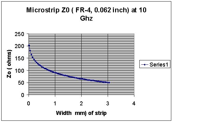
Microstrip characteristic impedance for FR-4 at 10 Ghz
The characteristic impedance of microstrip changes at frequency owing to changes in the effective permittivity of the substrate. We analyzed this at 10 Ghz for a 0.062 inch substrate, with 1 oz copper and plotted the curve for Z0 ( characteristic impedance) change versus width of the microstrip. This is shown below. For more information on this and other interesting topics please visit the Signal Processing Group Inc. website.
Current carrying capability of a PCB Trace – addendum
This is an addendum to the original post on the current carrying capability of a PCB trace. The units of the width of the PCB trace were inadvertently left out. The units of the calculated width of the trace are mils.
Thickness of copper for given weight of copper on a PCB
A really fundamental parameter for PCB design is the copper weight to be used and the thickness of that copper. This post simply calls out these parameters for PCB designers who may need these constantly.
The thickness of 1 oz copper is 1.37 mils or 0.0347 mm
To determine the thickness of ( for example) 4 oz simply mutiply 1.37 mils by 4.0 ( or 0.0347 mm by 4.0). In terms of microns the thickness of 1 oz copper is 34.79 microns.
Please visit the Signal Processing Group Inc., website for more technical information, software, whitepapers etc.
MOSFET Flicker noise calculator
The flicker noise of MOSFETs, a low frequency noise phenomenon is well known, and is a limiting factor in analog MOSFET circuit design, specially for low frequencies. Most standard simulators include this in their subroutines. However, even before using these subroutines, it behooves the engineer to know what to expect. i.e which way the noise goes with variations in basic parameters of the MOSFET. In order to facilitate this Signal Processing Group Inc has released a Javascript calculator that is easy to use and provides reasonable results. It is based on a paper already released by SPG that can be found under the menu item ” Download white papers, articles and freeware” in the Signal Processing Group Inc. website. Interested readers can find these items there.
s11 ( reflection coefficient ) to impedance conversion for simulation
s11 is the input reflection coefficient expressed in terms of s – parameters. It can be used as is in certain software programs to analyze the input characteristics of a 2 – port circuit. However, if these specialized programs are not available then a conversion between s11 can be carried out from the known ( measured) value of s11 using either the Smith Chart or by using a simple calculator for the conversion. The basic conversion algorithm is as follows:
Z = Zo * ((1 + Γ) / (1 – Γ))
Γ = (Z – Zo) / (Z + Zo)
S11 = 20 * Log10(mag)
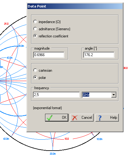
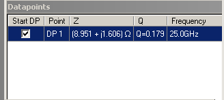
Here Z is the impedance corresponding to the reflection coefficient, Zo is the characteristic impedance, Γ is the reflection coefficient. Obviously the calculations involve complex numbers as the impedances and the reflection coefficient are all complex numbers. Another way to do the conversion is to use the Smith Chart. As shown below. Just input the value of s11 or the reflection coefficient and read the impedance at that point..The example below converts a s11 magnitude of 0.6966 and angle 176.2 to an equivalent impedance directly.
The Smith Chart program used here is a freeware program developed by Prof. Fritz Dellsperger , Juerg Tschirren and Roger Wetzel of the Berne Institute of Engineering and Architecture.
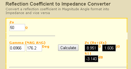
The same function can be done using a calculator as mentioned above. The results of the calculator are shown below:
The calculator used for this function was from Le Leivre.com on the web. Please visit the Signal Processing Group Inc., website for more technical information, white papers, and general information for our cost – effective design, development and manufacturing services for Analog and RF/wireless ASICs and modules.
Impedance matching simulations using PSPICE
Impedance matching is a critical skill required for a large number of electronic circuit designs. A number of popular techniques are used over and over again and many are inbuilt into certain software packages. However, if one wishes to check out the matching using an independent package like PSPICE it becomes interesting to see what impedance matching means in the PSPICE domain. This allows the designer to check and re-check his design with a simple tool that is freely available in the industry, both as freeware and as a purchasable package with many “bells and whistles”. Ultimately though it is engineering judgement that counts and a simple way to check one’s work is always desirable. Please visit the Signal Processing Group Inc., website and check under the ” free articles…” menu item for an article addressing the impedance matching simulation technique and its interpretation.


